

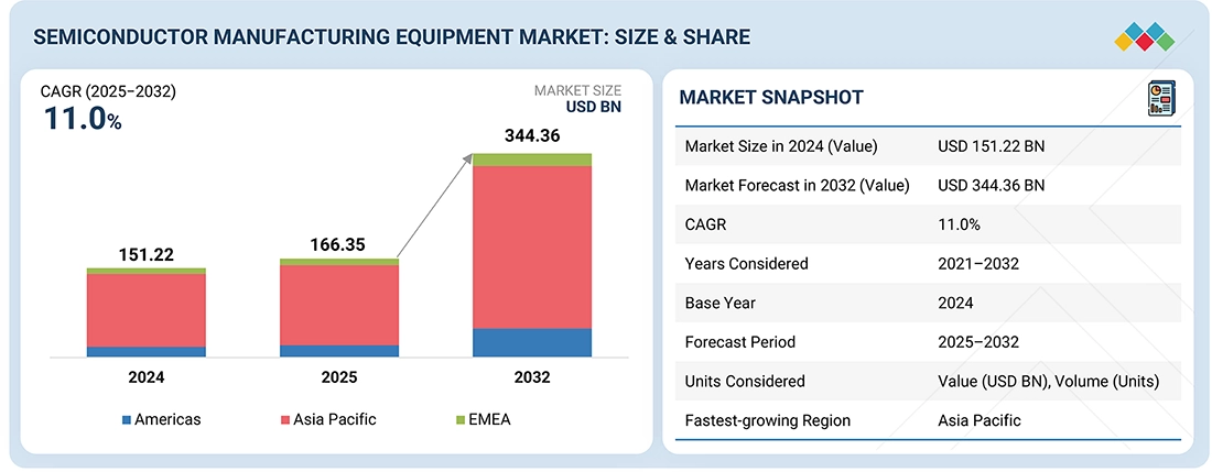
DELRAY BEACH, FL. – August 31, 2026 – The report “Semiconductor Manufacturing Equipment Market by Lithography, Wafer Surface Conditioning, Wafer Cleaning, Deposition, Assembly & Packaging, Dicing, Metrology, Bonding, Wafer Testing/IC Testing, Memory, Logic, Discrete, Analog – Global Forecast to 2032” The global semiconductor manufacturing equipment market is projected to reach USD 166.35 billion in 2025 and USD 344.36 billion by 2032, exhibiting a CAGR of 11.0%. A major factor driving the semiconductor manufacturing equipment market is the surging demand for advanced-node chips used in AI-powered devices, high-performance computing devices, 5G devices, medical electronics, and automotive systems. As chipmakers transition to smaller geometries, such as 5 nm, 3 nm, and the upcoming 2 nm nodes, they require highly sophisticated lithography, deposition, etching, and metrology tools, which significantly increase capital spending on advanced semiconductor equipment.
Download PDF Brochure @ https://www.marketsandmarkets.com/pdfdownloadNew.asp?id=263678841
Browse 170 market data Tables and 80 Figures spread through 271 Pages and in-depth TOC on “Semiconductor Manufacturing Equipment Market”
View detailed Table of Content here – https://www.marketsandmarkets.com/Market-Reports/semiconductor-manufacturing-equipment-market-263678841.html
Deposition Equipment Segment to record highest CAGR of Front-end Semiconductor Manufacturing Equipment Market during forecast period
The deposition equipment is projected to record the highest CAGR of the front-end Semiconductor Manufacturing Equipment Industry during the forecast period due to its critical role in enabling advanced-node device fabrication and emerging chip architectures. As technology nodes scale to 5 nm, 3 nm, and 2 nm, semiconductor structures require increasingly complex thin films, multi-layer stacks, and new materials to support higher performance, lower power consumption, and improved reliability. This drives strong demand for advanced physical vapor deposition (PVD), chemical vapor deposition (CVD), and atomic layer deposition (ALD) systems, particularly ALD, which offers atomic-level precision essential for gate-all-around (GAA) transistors, 3D NAND, and heterogeneous integration. Additionally, the rise of 3D architecture, chiplet-based designs, and advanced packaging further expands the need for thin-film deposition. Continuous innovation in materials engineering, combined with the growing adoption of high-performance devices across AI, HPC, automotive, and 5G applications, reinforces the rapid growth trajectory of deposition technologies, making them the fastest-expanding segment in front-end equipment.
Packaging Equipment Segment to register highest CAGR in Back-end Semiconductor Manufacturing Equipment Market between 2025 and 2032
The packaging equipment segment is expected to register the highest CAGR in the back-end semiconductor manufacturing equipment market, driven by the accelerating shift toward advanced packaging technologies that enable higher performance, greater functionality, and improved energy efficiency. As devices transition to 2.5D and 3D architectures, chiplets, heterogeneous integration, fan-out wafer-level packaging (FOWLP), and high-bandwidth memory (HBM) become increasingly complex. These next-generation architectures require highly precise die bonding, thermal management, underfill, bumping, and wafer-level packaging tools, driving significant capital investments. Additionally, AI, HPC, automotive electronics, and 5G systems increasingly rely on advanced packaging to achieve higher density and faster interconnects, thereby amplifying the demand for innovative packaging solutions. The combination of rising integration requirements, the adoption of new materials, and the expanding use cases across high-growth end markets positions packaging equipment as the fastest-growing back-end segment during the forecast period.
Inquiry Before Buying @ https://www.marketsandmarkets.com/Enquiry_Before_BuyingNew.asp?id=263678841
Americas to exhibit highest CAGR in global Semiconductor Manufacturing Equipment Market from 2025 to 2032
The Americas, led by the US, is expected to exhibit the highest CAGR in the semiconductor manufacturing equipment market due to strong government-backed initiatives, aggressive fab expansion plans, and strategic investments from leading global chipmakers. The US CHIPS and Science Act has triggered substantial capital inflows to build new fabrication facilities and modernize existing ones, attracting major players such as Intel, TSMC, Samsung, Micron, GlobalFoundries, and multiple memory and advanced packaging developers. The region has rapidly scaling capacity for advanced logic, AI accelerators, and heterogeneous integration, driven by rising demand from data centers, defense, automotive, and high-performance computing sectors. Additionally, the Americas is strengthening its domestic supply chain through partnerships across materials, metrology, and equipment manufacturing, further accelerating equipment procurement. This surge in regional manufacturing activity, coupled with long-term strategic efforts to localize semiconductor production, positions the Americas as the fastest-growing market for semiconductor manufacturing equipment over the forecast period.
Applied Materials, Inc. (US), ASML (Netherlands), LAM RESEARCH CORPORATION (US), Tokyo Electron Limited (Japan), and KLA Corporation (US) are the key players in the Semiconductor Manufacturing Equipment Companies.
About MarketsandMarkets™
MarketsandMarkets™ has been recognized as one of America’s Best Management Consulting Firms by Forbes, as per their recent report.
MarketsandMarkets™ is a blue ocean alternative in growth consulting and program management, leveraging a man-machine offering to drive supernormal growth for progressive organizations in the B2B space. With the widest lens on emerging technologies, we are proficient in co-creating supernormal growth for clients across the globe.
Today, 80% of Fortune 2000 companies rely on MarketsandMarkets, and 90 of the top 100 companies in each sector trust us to accelerate their revenue growth. With a global clientele of over 13,000 organizations, we help businesses thrive in a disruptive ecosystem.
The B2B economy is witnessing the emergence of $25 trillion in new revenue streams that are replacing existing ones within this decade. We work with clients on growth programs, helping them monetize this $25 trillion opportunity through our service lines – TAM Expansion, Go-to-Market (GTM) Strategy to Execution, Market Share Gain, Account Enablement, and Thought Leadership Marketing.
Built on the ‘GIVE Growth’ principle, we collaborate with several Forbes Global 2000 B2B companies to keep them future-ready. Our insights and strategies are powered by industry experts, cutting-edge AI, and our Market Intelligence Cloud, KnowledgeStore™, which integrates research and provides ecosystem-wide visibility into revenue shifts.
Media Contact
Company Name: MarketsandMarkets™ Research Private Ltd.
Contact Person: Mr. Rohan Salgarkar
Email: Send Email
Phone: 18886006441
Address:1615 South Congress Ave. Suite 103, Delray Beach, FL 33445
City: Delray Beach
State: Florida
Country: United States
Website: https://www.marketsandmarkets.com/Market-Reports/semiconductor-manufacturing-equipment-market-263678841.html
Press Release Distributed by ABNewswire.com
To view the original version on ABNewswire visit: Latest Research on Metrology in the Semiconductor Manufacturing Equipment Market by MarketsandMarkets™


